Laser Debonding Equipment Market Trends & Future Outlook, 2033 | UnivDatos
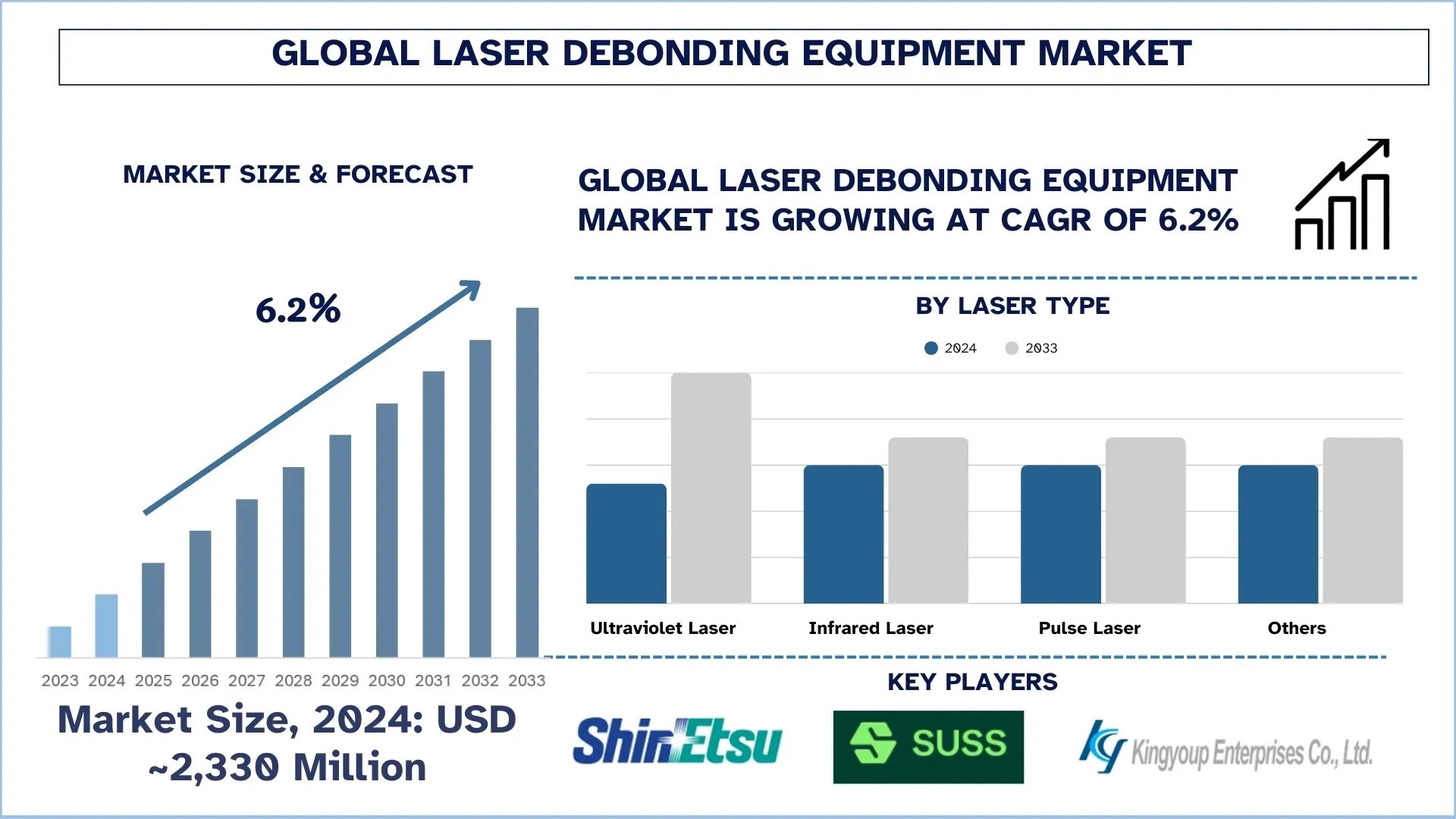
The Global Laser Debonding Equipment Market was valued at USD 2,330 million in 2024 and is expected to grow to a strong CAGR of around 6.2% during the forecast period (2025-2033), owing to the increasing demand from the end-user industries for advanced packaging solutions. Newer advanced technologies such as AI, automation, and smart manufacturing systems have further spurred the demand for precision non-contact debonding processes. Laser debonding systems fulfill these very requirements, with low substrate damage, making them well-suited for current high-density packaging and wafer thinning applications.From a market value perspective, the laser debonding equipment market is estimated to reach USD million by 2033, progressing at a stable CAGR of 6.2%. The increased scalability of AI systems and types of laser technology, such as ultrafast laser pulses and laser beam shaping technology, are heavily accelerating laser debonding equipment adoption. In addition to this, growth in cloud-based infrastructure, generative AI applications, and real-time process monitoring are fueling wider deployment of systems within the manufacturing value chain. Government-enabled initiatives that support domestic semiconductor production and a growing emphasis on cleanroom-compatible, high-yield production lines are also set to contribute to market growth.
Access sample report (including graphs, charts, and figures): https://univdatos.com/reports/laser-debonding-equipment-market?popup=report-enquiry
Shin-Etsu Engineering Co., LTD:
Shin-Etsu Engineering Co., Ltd., known as a subsidiary of Shin-Etsu Chemical Co., Ltd., makes advanced semiconductor processing equipment with a special focus on laser debonding and cleaning technologies. The SELD-LASER Series uses a 355 nm pulsed laser licensed from IBM to accurately peel off temporary bonding layers without creating stress, which makes the laser suitable for ultra-thin semiconductor applications. Periodically cleaning the residues from the temporary bonding layers created during laser debonding is one of the applications in which the wet cleaning solutions of the SELD-Cleaner Series contribute to improving process expediency. Such systems are crucial in the FOWLP and RDL formation processes in microelectronics and micro-LEDs.
EV Group (EVG):
EV Group (EVG) is known for its cutting-edge solutions in semiconductors and MEMS manufacturing, with laser debonding technology being a core competence. The EVG®850 DB Automated Debonding System employs fully automated operations to separate and clean processed temporary bonding wafer stacks. It is characterized by real-time monitoring and recipe-controlled processes, capable of processing substrates of up to 300 mm diameter. The EVG®880 LayerRelease™ System also relies on infrared laser technology for nanometer precision in layer release from silicon carrier substrates, thus enabling advanced 3D integration and heterogeneous device manufacturing.
SUSS MicroTec SE:
SUSS MicroTec SE, together with its subsidiaries, develops, manufactures, markets, and maintains systems to produce microelectronics, microelectromechanical systems, and related applications. It operates in two divisions: Advanced Backend Solutions and Photomask Solutions. The company offers mask aligners, coaters and developers, UV projection scanners, and temporary and permanent bonders for advanced packaging, microelectromechanical systems, compound semiconductors, and 3D integration markets. It also provides specialized systems for the cleaning and processing of photomasks for the semiconductor industry. The company operates in Europe, the Middle East, Africa, North America, and the Asia Pacific. It distributes its products through production facilities, as well as through distribution companies and trade representatives. SUSS MicroTec SE was founded in 1949 and is headquartered in Garching bei München, Germany.
Click here to view the Report Description & TOC: https://univdatos.com/reports/laser-debonding-equipment-market
CWI Technical:
CWI Technical is a company that has specialized in providing precision equipment for semiconductors and microelectronics manufacturing for some time now. They have solutions for wafer thinning and temporary bonding processes that are essential to laser debonding applications, among others. There are not many details about their laser debonding tool, but because of their competence in matters related, one can argue that they are a worthy player in the semiconductor processing ecosystem, wherein laser debonding is finding increasing relevance with device miniaturization and performance enhancement. CWI Technical specializes in precision equipment for semiconductor and microelectronics manufacturing. They have solutions for wafer thinning and temporary bonding processes that are essential to laser debonding applications, among others. However, specific information about their laser debonding equipment is scarce; however, because of their competence in related matters, they may be claimed to constitute an important player in the semiconductor processing ecosystem, where laser debonding is becoming more relevant with the miniaturization and performance enhancement of devices.
Kingyoup Enterprises Co., Ltd:
Kingyoup Enterprises Co., Ltd., based in Taiwan, manufactures precision machinery for the semiconductor field. They provide a range of solutions for wafer handling and processing, particularly laser debonding applications. Their equipment involves temporary bonding and debonding processes that are essential for advanced packaging processes like 3D ICs and FOWLP. Some specific information regarding their laser debonding systems is not readily available; however, their products aim to facilitate wafer handling and processing, which are needed for advanced semiconductor manufacturing that is more and more becoming reliant on laser debonding technologies.
Contact Us:
UnivDatos
Contact Number - +1 978 733 0253
Email - contact@univdatos.com
Website - www.univdatos.com
Linkedin- https://www.linkedin.com/company/univ-datos-market-insight/mycompany/
The Global Laser Debonding Equipment Market was valued at USD 2,330 million in 2024 and is expected
Share: